|
To Irina in her birthday
REVIEW
DIGITAL DEVICES BASED ON COMPLEMENTARY JUNCTION FIELD EFFECT TRANSISTORS
PREAMBLE
Now CMOS transistors are widespread component basis for digital integrated circuits. But its have a disadvantage that is high sensitiveness to environment effects such as temperature and radiation. The disadvantage restrains using CMOS IC in electronics equipment worked in extremal conditions.
There is a alternative component basis that is junction field effect transistors (JFET) which possesses more high resistance to environment effects. The cause of the stability is physical nature of JFET, namely electric charges are carried by majority carriers and in a depth of semiconductor as opposed to CMOS transistor, which has a current, carried by minority carriers and on surface of semiconductor. JFET is appropriate to base element of radiation hardened Integrated Circuits.
Complexity and inefficiency schematic methods of JFET logic gate design do not allow widely using JFET in area of digital IC. There is a fact that JFET gate's control voltage has a polarity that is reversal of polarity of drain voltage. That fact results in necessity to have two voltage supply sources and complex schemes of a matching of a logic level voltage between JFET gate's inputs and outputs.
Given review introduces schematic methods of developing of a logic gates based on complementary JFET (CJFET) that are free against above disadvantages. Namely, it works with only one voltage supply source, without shift of logical level of voltage between gate's input and output. And the CJFET gates have micro-power ability, the same as CMOS gates: its work without power drain in static states.
1. LAMBDA-DIODE - BASIS COMPONENT OF CJFET LOGIC GATES
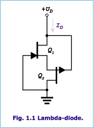
Two-terminal device composed of n-channel and p-channel JFET, as shown in fig. 1.1 has the characteristic similar to the lambda-diode [1]. Volt- ampere characteristic of the two-terminal device (we will call it lambda- diode then) is shown in fig. 1.2.
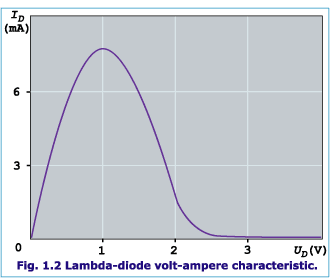
Similarly to the usual semiconductor diode, the lambda-diode has two states: it is conducting (impedance to tend to null) and it is not conducting (impedance to tend to infinity). As well as the usual diode the lambda- diode in the not conducting state has a current close to 0 and defined by leakage current, but in the conducting state lambda-diode has a essentially differ characteristic (see fig. 1.3).
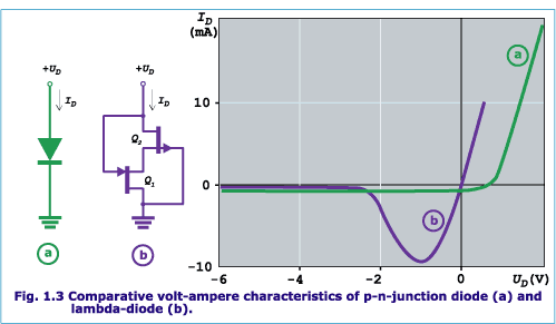
To keep a usual diode in conducting state a one needs a forward-bias voltage equals 0.5 - 0.7 V and accordingly there is necessary to provide for a significant current through it. A lambda-diode does not need a forward-bias voltage, it is conducting with voltage equals 0V and has no a current through it in this state. This is very important for realizing of micro-power logic gates.
It is necessary to note, that the lambda-shaped branch of volt-ampere characteristic does not prevent operation of the device as a diode, but only improves its dynamic characteristics.
2. DIODE LOGIC CIRCUITS
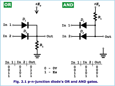
Let's consider examples of 'OR' and 'AND' logic gates developed with lambda-diodes, by analogy to semiconductor diodes (see fig. 2.1).
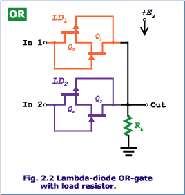
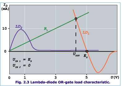
The logic gate OR constructed on lambda-diodes is shown on fig. 2.2 and fig. 2.3 represents the load characteristic of the device. Apparently from diagrams, if any input (or both) has a high level voltage (Es), then output has a high voltage too and it closes to Es (logical '1'), because lambda-diode with voltage equals Es on its terminal is conducting. The current passing through lambda-diode and load resistor makes output voltage equals to '1' logic level (~Es). Further, if another input of the gate has a low level voltage (0V), corresponding lambda-diode comes to non-conducting state and has no effect to gate's state.
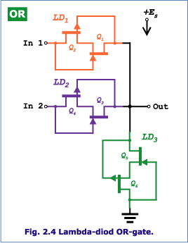
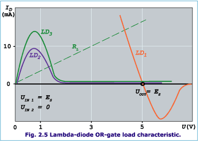
The disadvantage of this circuit is current through the conducting lambda-diode and the load resistor, but it can be easy corrected by replacing the resistor on one more lambda- diode (see fig. 2.4). Load characteristic of the device shown on fig. 2.5 indicates that lambda-diode connected instead of load resistor avoids a static current through the gate.
The 'AND' gate can be similarly created as shown in fig. 2.6.
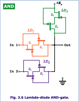
Note, to build a valuable logic devices of any functional complexity it is necessary to add to the given set a logical inverter and a buffer amplifier. Further it is shown, that these devices are easily realized within a bounds of considered schematic design.
3. TRANSPONDER-AMPLIFIER AND INVERTER BASED ON CJFET
If connection of a gate circuit of a lambda-diode's JFET has broken and has fed control voltage to the gate we get a three-pole device which logically to call lambda-transistor [2]. There are two types of the three pole devices or lambda-transistors and one is shown in fig. 3.1. It has volt-ampere characteristics those are similar to characteristics of a MOS transistor. Another type of a lambda-transistor is shown in fig. 3.2.
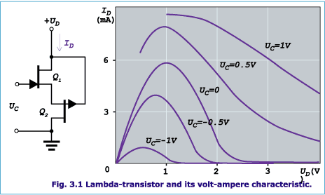
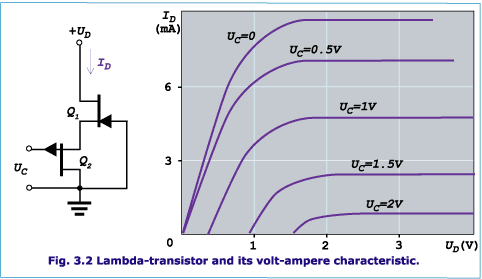
Notice that gate control voltage and drain voltage have some limitation associated with necessity to avoid forward-bias gate-channel voltage of field-effect transistors that formed lambda-transistor. It is important that control voltage and drain voltage of a lambda-transistor have the same polarity in contrast to single field-effect transistor. The fact allows creating devices like CMOS logic.
A schematic circuit of the transponder-amplifier is shown on fig. 3.3. The both shoulders (upper and lower) of the transponder is a lambda-transistors of the second type (fig. 3.2) and have the same type of control, but they have opposite conductivity of a FETs formed a lambda-transistors. The fig 3.3 also represents a load characteristic of the device. The diagram clearly shows that one of lambda-transistors is not conducted in any of state of the repeater and does not allow running a current from a power supply source. Let's see how it work in detail.
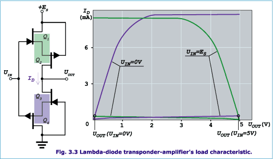
Suppose input voltage equals 0V ( '0' logic level ). The lower lambda-transistor is in conducting state (see VA diagram on fig. 3.2 with Uc=0V) but upper lambda-transistor is in nonconducting state (see VA diagram on fig. 3.2 with Uc>2V). Output voltage equals 0V with this condition. Note there is no current throw the device - upper lambda-transistor is off and has only leakage current, but lower one is on and keeps low level of output. Because the circuit is symmetric we have the same situation in static state with input voltage equals Es. When input level is changing from 0V to Es a output capacitance is re-charging by current of on upper lambda-transistor and vice versa a output capacitance is re-charging by current of on lower lambda-transistor when input voltage is coming from Es to 0V.
In a similar way[3,4], it is possible to design the logical inverter, (see fig. 3.4). Here the both shoulders of the inverter is a lambda-transistors of a first type (fig. 3.1.). This lambda-transistors have a complementary conductivity of forming FETs. When input level voltage equals 0V the upper lambda-transistor is on (see VA diagram on fig.3.1. with Uc>1V) and lower lambda-transistor is off (see VA diagram on fig.3.1. with Uc=0V). Output level voltage is high and equals Es. Then input voltage is high (=Es) the upper lambda-transistor is off and lower lambda-transistor is on, so output voltage equals 0V.
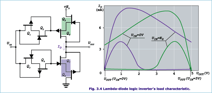
This device has a problem: lambda-transistor in conducting state has a forward-bias gate junction. To avoid running of a current through a gate, a lambda-diode is inserted in each lambda-transistor's control circuit as showed in fig.3.4 (Q1, Q2, Q3 and Q4). These lambda-diodes reliably disconnect forward-bias gate of the field-effect transistor, but in not conducting state of the lambda-transistor, its gate is connected through the conducting lambda-diode to a source of a control voltage. As well as the previous device, there is no power drain from a power supply source in a static state.
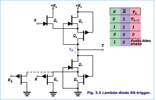
Moreover, memory cells and the flip-flop can be easily created by means of lambda-diodes [5,6,7]. Fig. 3.5 shows the schematic circuit of the RS-trigger. A basis of the trigger is two lambda-diodes, sequentially connected. The given circuit has two steady states - one lambda-diode is conducting, another is not conducting. Two additional field-effect transistors are for switching the trigger from one state to another. The gates of them are R (more precisely (NOT)R) and S input terminals of the trigger.
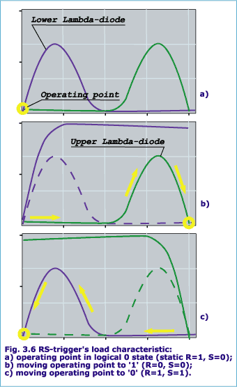
How it works? Suppose our trigger is in "0" logical stable state, output voltage equals 0 (see fig. 3.6, a), 'S'-input has level 0 and 'R'-input has level 1. The both shoulder lambda-transistors have a VA-characteristic showed in fig. 3.1, Uc=0V and operation point in position with opened lower lambda-transistor and closed upper lambda-transistor. When 'R'-input is assumed low level = 0V the lower lambda-transistor is obtained VA-characteristic showed in fig. 3.1, Uc=1V. After that operation point should move to other stable point as showed in fig. 3.6, b. The state is "1" logical state of the trigger with upper lambda-transistor is in and lower lambda-transistor is off. To switch the trigger to "0" logical state again we have to set 'S'-input to high level = 5V. Now the upper lambda-transistor is obtained VA-characteristic as showed in fig 3.6, c and operation point moves to previous "0" stable position. To control the trigger it is enough to feed RS-inputs short impulse with wide that allows to switch trigger to other stable state. After control impulse is over the trigger will keep its state until next control impulse comes.
If we insert additional transistors in parallel with control one we can get the 'AND' gate on input terminals Ri or Si as shown in fig. 3.5.
4. LAMBDA-DIODE LOGIC GATE BASED ON DEPLETION-TYPE MOSFET
A lambda-transistors described above have a significant obstruction. This is a possibility of control JFET's gate junction to obtain a forward-bias state. This possibility prevents to easily build CJFET logic gates. There is alternative variant: this is a using of depletion-type metal oxide semiconductor field effect transistor (MOSFET) for a lambda-diode and a lambda-transistor. A depletion-type MOSFET has the same a principle of operation and the same type of volt-ampere characteristics as a JFET but the MOSFET has a gate isolated from transistor's channel. The fact significant simplifies of a logical gate building in comparison with JFET in lambda-diode context.
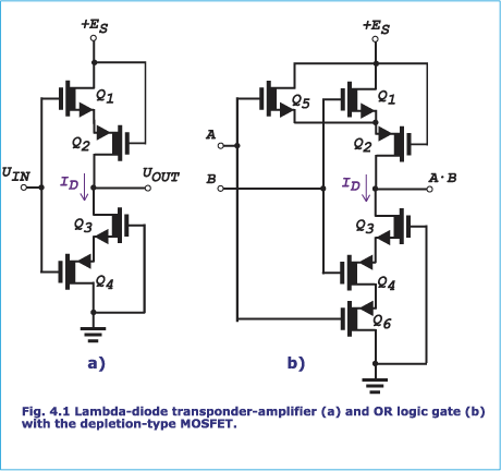 As a mentioned above a depletion-type MOSFET has the same characteristics as a JFET. This is a reason why schematic diagrams of a devices based on MOSFET look like a ones based on JFET. For example look at transponder in fig 4.1, a. It works the same way as transponder in fig. 3.3. Isolated gates of MOSFET allow us to build a logical gates similar CMOS gates. Let see in fig 4.1. b, here is logical gate 'OR'. If any of inputs (A or B) have a logical level '1' (U = 5V) the upper shoulder is in and lower shoulder is off. Output level is '1'. If both inputs (A and B) have a logical level '0' (Ua = Ub = 0V) the upper shoulder is off and lower shoulder is in. Output level comes to '0'.
Note we can not use the same schema with CJFET, because when transistor Q6 is off and Q4 is in, a forward-bias gate of Q4 (in JFET case) will break functionality of the device. To avoid this problem (in JFET case) we have to insert in a gate circuit of each control transistor a lambda-diode similar diagram in fig.3.4. Now with MOSFET we can eliminate this lambda-diodes.
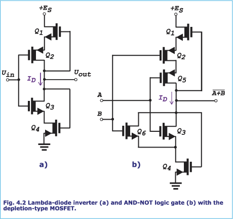 Next fig.4.2. shows realization of a depletion-type MOSFET inverter (a) and logical gate 'AND' (b).
Although a depletion-type MOSFET's implementation of a lambda-diode based logic circuits avoids a forward-bias gate problem and make easy of circuit design but a depletion-type MOSFET yields to JFET in temperature and radiation resistance.
5. IMPLEMENTATION OF JFET LAMBDA-DIODE
Let see how implement a described above devices as a microelectronics structures (a solid-state circuit). Limit our discussion of a describtion of lambda-diode construction as a base element of CJFET circuits shown above. There is a few variant of technology implementation of a lambda-diode, the most simple one is standard epitaxial-planar process.
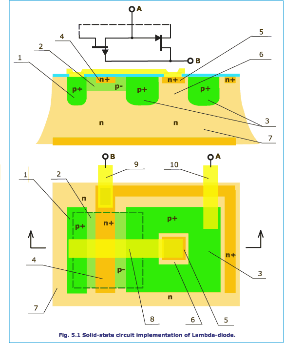 Fig 5.1. shows construction of lambda-diode. JFET with p-channel is represented on left side of the diagram. On the right side it is a n-JFET with vertical orientation of channel. The numbers on the figure mean as follows:
Note for implementation of more compose logical devices we need to isolate a separated JFET in lambda-transistors.
7. CONCLUSION
The devices considered in the review, similar CMOS logic have a low current drain from a power supply source in statical state. But they can not compete with CMOS transistor logic in running speed because the lambda- diode, the basic component of the considered schematic design has two sequentially connected channels of field-effect transistors, and CMOS logic only one.
But junction field-effect transistors with a channel in a depth of semiconductor have more stable characteristics in a temperature range and at high levels of radiation. It allows to apply integrated circuits on lambda- diodes in radiation hardened electronics equipment that is subjected to hard effects of environment, for example in space ships or in nuclear reactors equipment.
1 October 2003
REFERENCES
[1] Kano, G. The lambda diode: versatile negative-resistance device. "Electronics", 48(1975), N13, p.105-109.
[2] Basic elements for micro power integrated circuit based on field-effect transistor. "Izvestiy vuzov USSR". Radio electronics, 1982, v. XXY, N5. p.55-60. Sukchorukov A.I., Pereverzev A.V., Krasnopolski A.G.
[3] Inventor's certificate N 741473, "Junction field effect transistor's inverter", H03k 19/40, USSR, application for an invention 2689891 from 30.10.78, authors - Killmetov R.S., Krasnopolski A.G., Mekchanzev E.B., Pereverzev A.V., Sukchorukov A.I.
[4] Inventor's certificate N 953732, "Junction field effect transistor's inverter ", H03k 19/094, USSR, application for an invention 3263649 from 12.01.81, authors - Killmetov R.S., Krasnopolski A.G., Mekchanzev E.B., Pereverzev A.V., Sukchorukov A.I.
[5] Inventor's certificate N 1316507, "Semiconductor device with lambda-type characteristic", USSR, application for an invention 3928040 from 08.07.85, authors - Mekchanzev E.B., Killmetov R.S., Krasnopolski A.G., Sukchorukov A.I., Rysukchin G.V., Gavriluk V. I., Gavriluk G.I.
[6] Inventor's certificate N 1324537, "Semiconductor device with lambda-type characteristic", USSR, application for an invention 3925377 from 08.07.85, authors - Mekchanzev E.B., Killmetov R.S., Krasnopolski A.G., Sukchorukov A.I., Rysukchin G.V., Gavriluk V. I., Gavriluk G.I.
[7] Inventor's certificate N 1347153, "Field effect transistor's D-trigger", H03k 3/286, 3/353, USSR, application for an invention 3791897 from 20.09.84, authors - Mekchanzev E.B., Krasnopolski A.G., Rysukchin G.V., Sukchorukov A.I., Gavriluk V.I.
|

 H O M E P A G E
A L E X E I K R A S N O P O L S K I


